Optical Nanostructures in CMOS Technology

Optical nanostructures in CMOS technology concerns the ability to structure the metal surfaces employed within a modern semiconductor process at the nanometer scale in such a way that they allow complex color and/or polarization sensors to be manufactured at a reasonable price. This calls for an understanding of surface plasmon effects in metals and materials relevant to CMOS as well as the optics expertise to design filters – expertise that Fraunhofer IIS possesses. Fraunhofer IIS has also developed the capacity to optically model nanostructured metals, along with simulation and design capabilities for nanostructured color and polarization sensors.

Here you find more information about our services.

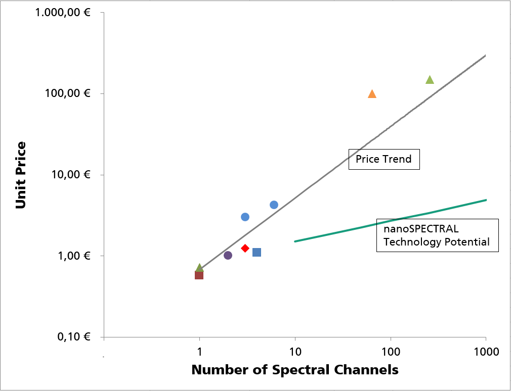
Distribution prices of different multispectral sensors compared to the costs using the nanospectral filter technology

Keyfacts and Benefits

Keyfacts

Benefits

  • Realization of many multispectral channels on one chip,
    with only 2 additional photolithographic process steps
  • Single-source manufacturing
  • Constant process costs for an arbitrary number of spectral channels
  • Metal filter material
  • Temperature resistance
  • Simple design of specific spectral behaviors
  • Application-specific filter properties
  • Applicable to existing single or image sensors
  • Easy implementation in standard products
  • Implementation in 2 different CMOS production plants
  • Independent service design and supply chains
  • Fast series transfer

Applications and technology potential

Lighting systems


  • Multispectral ambient light sensors
  • More spectral information compared to sensors with three channels
  • Integrated signal processing and standard interface I2C or SPI

Chip Size Spectrometer


  • Miniaturized multispectral sensors for the analysis of gases and liquids
  • Color sensors for industrial automation and automotive applications
  • Agriculture and smart farming

Multispectral imaging


  • Image sensors with spectral filters at the pixel level
  • Applying filters to standard products of new image sensors
  • Minimum pixel size: 5 μm