ntCT – forward thinking Nano CT

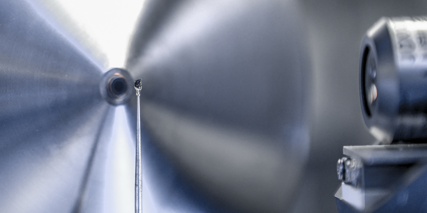
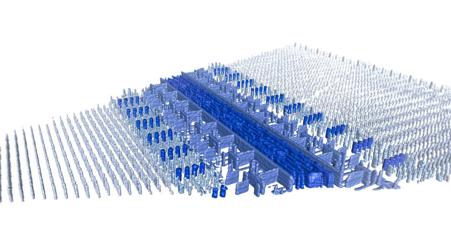
3D-computed tomography for the visualization of smallest structures

Siemens Star Test Chart. Smallest features of 150 nm lines and spaces.
The ntCT system.

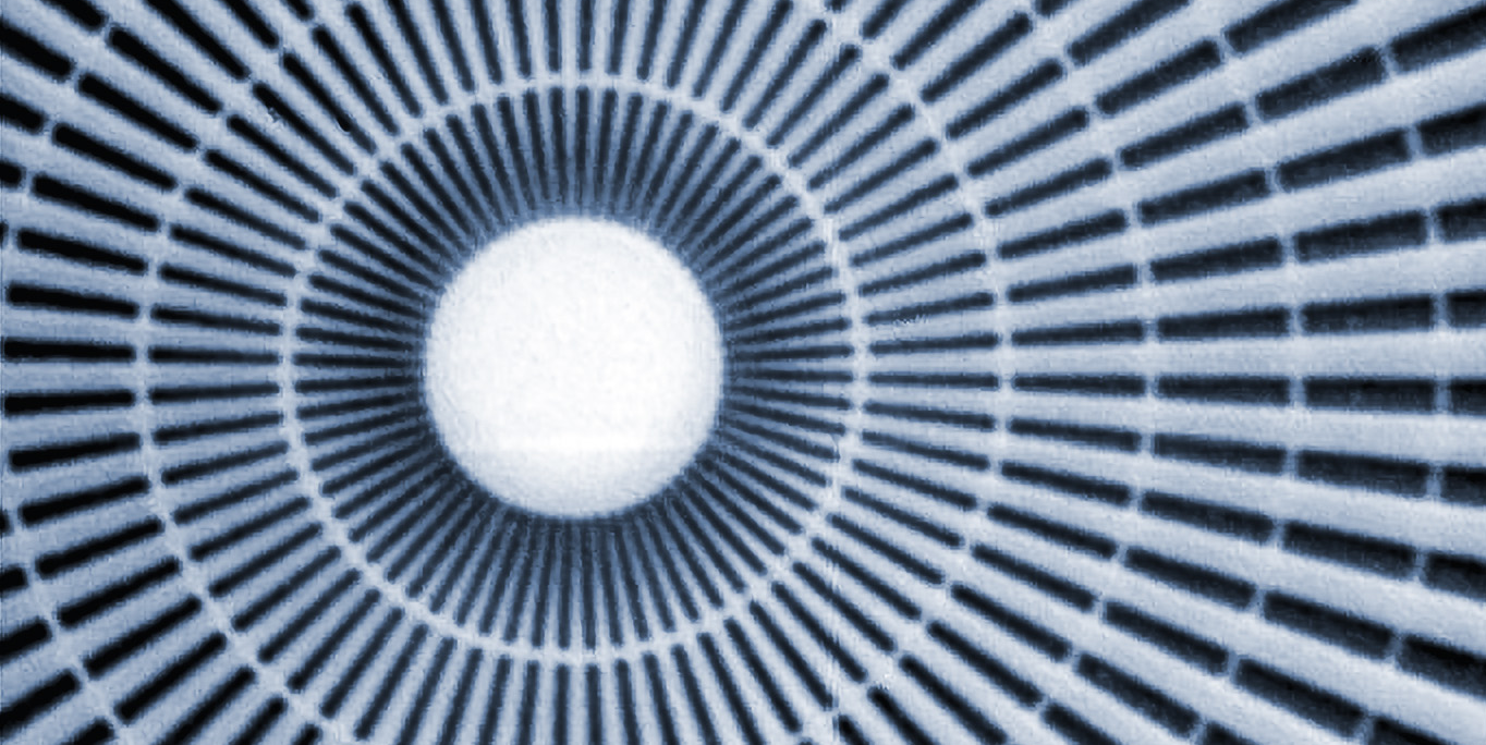
The functional features of novel material systems are often based on their complex inner structures, which are not accessible by established non-destructive analysis methods. The fabrication of microelectronics and micromechanics becomes more and more complex, packed and 3D. After decades of successful miniaturization, industry now produces structures too small for established process control, hindering further improvements. Moreover, biological investigations would require more detailed 3D information of hidden inner structures in order to understand the morphology of various organisms, but such samples often provide too low material contrast.

The ntCT provides a unique solution for all these high-resolution measurements far ahead of established industrial micro CT scanners by applying the latest developments from x-ray research.


  • Min. Voxel sampling 50 nm
  • Spatial resolution down to 150 nm
  • Energy down to 4 keV
  • Photon counting detector
  • Variable field of view
  • Automatic sample alignment
  • State-of-the-art reconstruction
  • Fully customizable


  • NDT and inspection of electronics
  • Investigations on microscopic structures in life sciences (microbiology, botany, etc..)
  • Research in new materials (filters, batteries, paper, etc..)
  • Cultural heritage

State-of-the-art components merged into a unique synthesis

© Fraunhofer IIS
NanoTube N2, a 60 kV X-ray tube with tungsten-diamond transmission target.
© Fraunhofer IIS
Cutting edge direct photon counting detector system.

Our experience in both hardware and software design enables us to perfectly adapt systems to your individual needs. Besides using only high-precision components, we also develop state-of-the-art reconstruction algorithms. The Swedish company Excillum is a specialized manufacturer of high performance X-ray sources. Excillum’s NanoTube N2, a 60 kV X-ray tube with latest tungsten-diamond transmission target technology, automatic e-beam focusing and astigmatism correction, ensures that the smallest possible, truly round X-ray spot is achieved.

The Swiss company DECTRIS is the most experienced company in photon counting X-ray detectors, which feature several advantages compared to commonly used flat-panel detectors. Most importantly, zero readout noise and zero dark current enable an optimum signal-to-noise ratio. Thus, the dynamic range of our X-ray radiographies is not limited by the detector. Moreover, dual energy discrimination enables digital spectrum adjustment.

Continuous developments

CT slices of an SD Card with 200 nm sampling. The upper scan was made with the Nanotube N1 in 15 h while the lower scan took only 4 h with the Nanotube N2.

Thanks to the close cooperation with the Swedish company Excillum AB, the X-Ray Source – one of the core components of the system – has now been upgraded to the next generation. This development goes hand in hand with numerous further improvements of the overall system by the Fraunhofer researchers. The result is a significant increase in performance, allowing to reduce the required scan times by a factor of 3 while maintaining the extraordinary resolution.

Application Examples

Biological samples – C. elegans, Voxel sampling: 450 nm.
Electronics – SD card, Voxel sampling: 200 nm.
© Fraunhofer IIS
Materials – Lithium anode, Voxel sampling: 140 nm.

Easy-to-use

An easy-to-use and intuitive Graphical User Interface is guiding the user throughout the whole workflow.

The control software supports the user in all matters. From an automated sample adjustment to setting the scan parameters to the reconstruction of the volume the user is guided by an easy and cleaned-up graphical user interface.

Specifications

Performance

Mechanics

Resolution

150nm

Sample stage

4 degrees of freedom (DOF)

Smallest sampling

50nm

Sample adjustment

2 DOF

Variable Field of View

100µm – 10mm

Detector stage

3 DOF

Max. Magnification

1500

Max. sample weight

200g


System footprint

2.2 x 1.2 m


Detector

Source

Pixel size

75µm

Min. X-Ray spot size

300nm

Accept. photon energy

4 keV – End of source spectrum

Acc. voltage

60kV / 110kV


tungsten-diamond transmission target


Environmental requirements


Dry air


Temperature stability of ± 0.7° K


Cooling water (optional)


Further information