ASIC Foundry Services

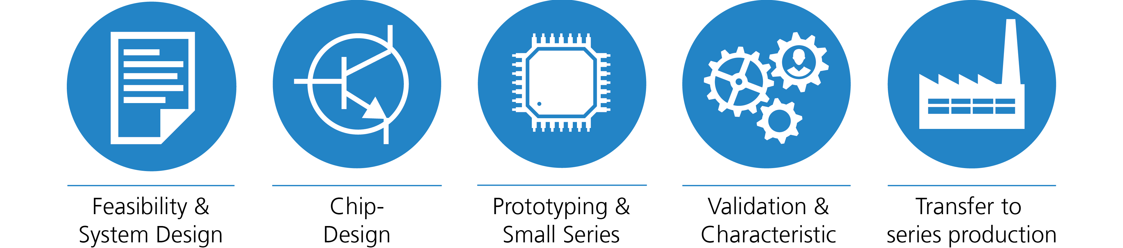
The Fraunhofer IIS has specialized in offering ASICs in small volume. Packaged and tested ASICs are available in quantities of a few hundred.
We are the interface to foundries and your supply chain partner from design to production.
We offer: IC specification, complete design flow (implementation of design concept), design of analog/digital systems and mixed signal applications, layout and verification (synthesis, place & route).

In the business field ASIC Foundry Services we handle volumes from 25/50 samples up to fabrication lots.
We offer: ASIC prototypes, ASICs in a low number of pieces (small volume), assembly, transfer to production, support for series test and full supply chain service.


Europractice

The European Commission launched the EUROPRACTICE initiative in October 1995 with the goal of helping companies to become more globally competitive through the availability of cost-effective ASICs, multichip modules (MCM) or microsystem solutions. The EUROPRACTICE IC Service furthermore offers European industry and academic institutions a safe path towards ASICs with following benefits:

  • Completely supported low-cost prototype production
  • Small-volume production
  • Fast production schedules
  • Wide selection of technologies
  • Supply chain services

Small-Volume Projects

EUROPRACTICE/Fraunhofer IIS initiates hundreds of small-volume projects, delivering some million ASICs. Customer demand ranges from 200 chips up to one million ICs. The average project volume is around 50,000 chips. For manufacturers however, 50,000 ASICs equate to an insignificant number of wafers, as it takes only 25 twelve-inch wafers to manufacture 250,000 chips with an area of 7 mm².

Prototyping and small volume IC Services

By using a Multi-Project Wafer (MPW) approach individual customer designs are pooled together for manufacturing, in order to share production costs. Each customer receives samples of its own prototype and has to pay only according to a fixed price list. In addition, we offer ASICs in small-volume batches and provide services for engineering runs and fabrication lots.
 

Prototypes Small-volume Batches Engineering Run Fabrication support

MPW

MPW with additional volume

Single-tooling with own mask set

Up to 50 Samples

100 – 1k

Approx. 6 Wafer

Lots of 25 Wafer

DRC (design rule check); ERC (electrical rule check); DfM (Design for Manufacturing)

Optional prototype assembly/packaging

Optional Assembly, Test, Qualification, Supply Chain Management

price list

on request

Request template

Foundries supported by Fraunhofer IIS

Multi-Project-Wafer- and Small-Volume-Logistics:

© EUROPRACTICE
EUROPRACTICE Technology Trends in the period 2009-2019
© Fraunhofer IIS
Technology Nodes via Fraunhofer IIS 2018-2019

We have longstanding partnerships with various semiconductor manufacturers as part of the EUROPACTICE program. We offer customers cost-effective access to current technologies through our foundries at ams AG, GLOBALFOUNDRIES, IHP, X-FAB:

  • CMOS
    ams: 350 nm - 180 nm
    GLO
    BALFOUNDRIES: 130 nm - 12 nm
    X-FAB: 180 nm – 130 nm
  • High Voltage CMOS
    ams: 350 nm - 180 nm
    GLOB
    ALFOUNDRIES: 130 nm
    X-FAB: 350 nm – 180 nm
  • High Speed SiGe
    ams: 350 nm
    GLOBALFOUNDRIES: 130 nm
    IHP: 250 nm - 130 nm
  • RF-SOI
    GLOBALFOUNDRIES: 45 nm
    X-FAB: 130 nm
  • Silicon Photonics
    GLOBALFOUNDRIES: 45 nm
    IHP: 250 nm

ams 0.35 μm
PROTOTYPING AND VOLUME PRODUCTION


Through EUROPRACTICE-IC, customers from academia and industry can gain access to Multi-Project-Wafer runs and Volume Production services of ams.


The ams state-of-the-art 8-inch fab is offering high-performance process technologies with more than 30 years of experience in wafer processing. The PDK (Process Design Kit) provides all building blocks required to create complex analog mixed-signal designs.

The ams 0.35 µm technologies with standard CMOS, HV, SiGe and Opto Process, fabricated in Austria, offer affordable and easy access to prototyping and small volume services for academia and industry.


GLOBALFOUNDRIES 130, 55, 45, 40, 28, 22, 12 nm
PROTOTYPING AND VOLUME PRODUCTION


Through EUROPRACTICE-IC, customers from both academic and private sectors can access Multi-Project-Wafer and Volume Production services of GLOBALFOUNDRIES.

GLOBALFOUNDRIES, is a leading specialty foundry with a broad range of platforms and features, such as RF CMOS, FDSOI, RFSOI, SiGe, FinFET, SiPhotonics. Technology nodes are ranging from 350 nm down to 12 nm. Globalfoundries’ 22nm and 28nm nodes are fabricated in Dresden, Germany.

The GLOBALFOUNDRIES 22FDX® employs 22 nm Fully Depleted Silicon-On-Insulator (FD-SOI) technology that delivers outstanding performance at extremely low power with the ability to operate at 0.4V ultra-low power and at 1pA per micron for ultra-low standby leakage.


IHP 0.25 and 0.13 μm
PROTOTYPING AND VOLUME PRODUCTION


EUROPRACTICE-IC provides access to IHP SiGe:C BiCMOS Technologies for Multi-Project-Wafer Prototyping and Small Volume Production.

IHP offers research partners and industrial customers worldwide access to its powerful SiGe:C BiCMOS technologies. Several generations of high-speed SiGe Hetero-junction Bipolar Transistors (HBT) have been developed and integrated in 0.25 μm and 0.13 μm BiCMOS technologies.

The 0.13 μm BiCMOS process SG13G2 represents the fastest currently available SiGe HBT technology featuring peak fT / fmax values of 300 GHz / 500 GHz. These IHP technologies are especially suited for applications in the higher GHz bands, e.g. for telecommunications & broadband, radar and more.  

G25H5_EPIC is the monolithic integration of photonic devices, such as detectors and modulators, in the frontend of a Si-based integrated circuit technology that allows shortest interconnects between photonics and electronics, from which high-speed performance of Electronic-Photonic Integrated Circuits (EPIC) greatly benefit. This technology is especially suited for Optical Transceivers for 100G / 200G / 400 GHz applications.

X-FAB 0.35, 0.18, 0.13 μm
PROTOTYPING AND VOLUME PRODUCTION


EUROPRACTICE-IC offers Multi-Project-Wafer and Volume Production services of X-FAB to academic institutions togetherwith small and medium-sized enterprises.

X-Fab is a leading foundry group for analog/mixed-signal semiconductor applications, with six manufacturing sites in Germany, France, Malaysia and the USA. X-FAB has a combined capacity of around 94,000 eight-inch equivalent wafer starts per month.

Technologies are ranging from 1.0 to 0.13 µm mixed-signal CMOS, special SOI and MEMS long lifetime processes for automotive, industrial, medical and other applications


More Information

Foundry Day

25.4.2023 | Fraunhofer IIS

IHP Workshop

26.4.2023 | Fraunhofer IIS

ams OSRAM Training

26.4.2023/ 27.4.2023| Fraunhofer IIS

Schedule and Prices

  • MPW-Runs
  • Mini@sic-Runs

Europe secures Europractice services to European academia and industry until end 2021

Imec, the world-leading research and innovation hub in nanoelectronics and digital technologies and its partners STFC-UKRI, Fraunhofer IIS, CMP and Tyndall announced today that Europractice was selected and granted European funding as a H2020 project.

Press release imec