 Fraunhofer Institute for Integrated Circuits IIS
First-Time-Right Design with Much Shorter Development Cycles
Erlangen/Dresden, April 20, 2015: The »Intelligent IP Mixed Signal Design Flow« methodology developed by the Design Automation group at the Fraunhofer Institute for Integrated Circuits IIS offers an unparalleled degree of automation, especially for the otherwise time-consuming, error-prone analog portion of the design.

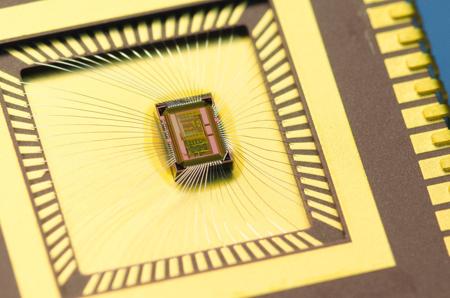
Integrated circuits that include both digital and analog elements, so-called mixed-signal ICs, are found in overwhelming numbers of today's microelectronic products, from consumer goods and critical automobile applications, to medical and aerospace systems. Although the analog circuitry usually accounts for no more than 20 percent of the chip surface, the low degree of automation leads to high development costs and risky designs, a problem that is exacerbated by the growing reliance on miniaturization in semiconductor technologies.
The »Intelligent IP Mixed Signal Design Flow« methodology developed by the Design Automation group at the Fraunhofer Institute for Integrated Circuits IIS now offers an unparalleled degree of automation, especially for the otherwise time-consuming, error-prone analog portion of the design.
Integrated circuit design: low-cost, fast and reliable
In several development projects, design engineers at Fraunhofer IIS were able to demonstrate significant improvements in efficiency by using intelligent IP mixed signal design flows. During the design of a multiphysical SMART sensor ASIC for instance, they reduced development costs and time by 40 percent. The result was the creation of various ASICs for different requirements in a single development cycle. Efficiency gains will eventually be realized even further through the automatic selection of the architecture during the system design. This innovative design flow was successfully used during the development of an industrial high-resolution A/D converter and an extremely fast image sensor. Johann Hauer, head of mixed signal ASIC development at IIS, has nothing but praise for the new methodology: »Although we have been striving for automated analog design processes for years, this complete design flow finally delivers the expected benefits for our daily development activities. A 40 percent reduction in development time and extremely reliable designs means that we can finally offer first-time-right designs with much shorter development cycles. Another key factor is the very high acceptance level among our design engineers due to the intuitive approach.« Customers who outsource the development of mixed signal ASICs and IPs to Fraunhofer IIS can reap the benefits of this new design flow today. Customers who develop their own integrated circuits can adopt the new design flow beginning in 2016.
One development cycle for multiple applications and different technologies
The design flow currently supports established production technologies from various manufacturers, from 350 nm to 28 nm. Even now, researchers are driving the further development of future ultra-low-power 28 nm technologies in several research projects with the aim of demonstrating their utility in microelectronic systems used in safety-critical automobile applications and aerospace cabin communications.