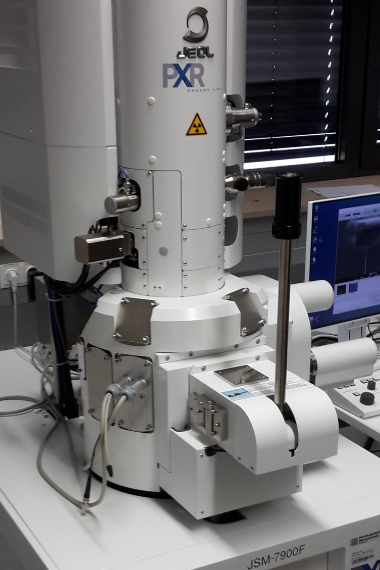
XRM-II nanoCT - Field-emission scanning based electron microscope

© Fraunhofer IIS
The XRM-II nanoCT is based on a field-emission scanning electron microscope, which is capable of a variable magnification range from 100x to 2000x.

The XRM-II nanoCT is a nano CT system based on a field-emission scanning electron microscope (SEM). A needle-shaped reflection target, which is installed inside the specimen chamber, in combination with the focusing electron optics of the SEM generate a x-ray spot of about 100 nm. A single-photon-counting direct-converting detector with a CdTe sensorlayer is used for x-ray detection. The system supports a variable magnification range from 100x to 2000x achieved by geometric magnification, which equals a voxel size between 600nm and 30nm.

Combination of SEM and nano CT

© Fraunhofer IIS
Nano CT; EDS; EDS (Cer); EDS (Zirkonum) Example of nano CT & EDS of a three-way-catalytic-converter

Despite additional installations for the nano CT, the complete functional range of the SEM is still available. Therefore the XRM-II nanoCT supports a combination of both, electron and x-ray imaging techniques in one system. An additional EDS-Detector for the SEM offers the potential of element determination of the investigated sample.

Key applications

  • microelectronic devices
  • metallic alloys
  • particles of Li-ion batteries
  • filter materials 

nanoCT

© Fraunhofer IIS
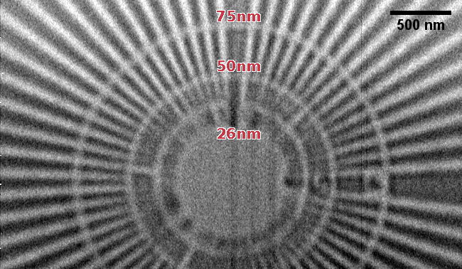
Resolution test pattern
  • magnification range: 100x - 2000x (voxel sampling: 600nm – 30nm)
  • resolution up to 50nm
  • acceleration voltage 5-30kV
  • 1-12mW power
  • photon-counting CdTe detector (55µm pixel-size)
  • different target materials: W, Mo, Cu, Pt, Ti

SEM

  • resolution up to 0.8nm at 30kV
  • “low-voltage”-imaging down to 10V
  • integrated EDS/EDX-System